


Today’s industrial solar cell technology is dominated by the “standard solar cell process” -a p-type silicon wafer, a phosphorus-doped emitter with a screen-printed front-side contact grid, an aluminum back surface field (BSF) and full-area metallization.
This “simple” BSF process has boosted the solar industry in the last two decades, transforming it from lab-scale pilot lines into an industry that produces several gigawatts per year.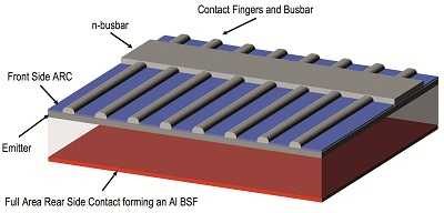
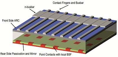
Lately, the PERC concept (“passivated emitter and rear contacts”) has received increased attention as a promising way to achieve higher solar cell efficiencies. PERC addresses the losses caused by the rear-side contacts through a dielectric passivation layer on the rear.The full-area contact previously used is reduced to points or lines where the coating is removed locally before metallization. It is expected that PERC will gain a significant market share in the coming years, mostly at the expense of BSF technology.
Several other future technologies are soon the be launched on the market– based on concepts that, like PERC, go back in time 20 years. Heterojunction (HJ) solar cells and interdigitated back contact (IBC) cells have already been mass-produced at some “pioneer” companies for years.Now, with dropping cell prices and lower margins, these old and at the same time new designs are again becoming the focus of the entire industry.
These three technology generations – BSF, PERC and the upcoming HJ and IBC cells – share many similarities regarding the requirements for optical inspection.However, there are also significant differences arising from the production philosophy for each technology.
Standard BSF technology
The BSF solar cell process can be considered the “working horse” process. The design is well understood, the processes are optimized, and all remaining efficiency losses due to design deficiencies are well researched. The art of making money with this type of solar cell lies in maximizing yield and throughput – speeding up handling and processing, reducing downtime to a minimum and running processes that remain stable in the event of variations in quality or changing material properties.
In particular, automated optical inspection for BSF technology must ensure robust performance at highest speeds. Requirements for the detection of special features such as sophisticated print patterns, low-contrast surface defects or smallest color variations are less crucial.Substantial defects must be sorted out reliably;minor underkill caused by shallow defects slipping through is more tolerable than overkill caused by pseudo defects. In short, automated optical inspection (AOI)needs to ensure consistently high performance and keep the production going – just like a working horse.
The big question is whether using an inspection system for process control can be beneficial in terms of production cost – or whether it reduces yield and throughput by adding complexity and potential downtime. The answer is two-fold: if the inspection system is well designed, it will allow for cost optimization in the process line, and pay back its investment in about six to nine months.“Good design” means hardware developed to ensure high availability, low maintenance effort, and short and rare maintenance downtime. A key feature for low maintenance is an internal calibration verification, which means that intervals for preventive maintenance and recalibration can be increased, and a fast calibration routine. Features like centralized recipe roll-out or offline recipe adjustment cannot play out as an advantage,as robust inspection systems in a stable BSF process do not require frequent recipe adjustments.
From standard BSF to PERC techn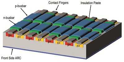 ology
ology
Even with standard BSF solar cells, changes to the print design allow for significant cost savings, e.g. through reduced paste consumption by printing perforated or hollow busbars. Other changes to the grid, such as reduced finger width, conical fingers, optimized redundancy lines, and 4 or even 5-busbar designs not only have the potential to save metal paste, but can also positively affect efficiency. For PERC cells, such optimizations and customizations of the front grid design have become the standard:custom designs optimize paste consumption, series resistance and tabbing adhesion, and provide uniqueness for increased memorability of a certain cell manufacturer.In addition, multi-wire concepts for connecting the cells in the module are evolving, adding new contact patterns to the already large variety of special front and rear metallization designs.
The special design features require increased flexibility to inspect different contact patterns.A crucial factor is that it is possible to configure the grid inspection without needing software code modifications from the supplier.An editor for easy and flexible print pattern design and a teach-in function to automatically extract the majority of settings from a cell image, or at least the possibility to import CAD designs into the editor are a must for fast development cycles and flexible, lean production. Still, every design must be inspected in less than 1 sec, which is a requirement that many toolbox-based software cannot fulfill.
 With PERC technology enabling a step up to higher efficiencies, the relevance of optical front-side quality increases. Dr. Eric Rüland, Managing Director of ISRA VISION / GP SOLAR,puts it in very clear terms: “Inspection becomes more and more important in solar industry. With high-efficiency PERC solar cells, no defects are accepted on the market – in contrast to standard BSF technology.” Even shallow defects must be sorted out reliably, as well as clusters of small defects, which – when treated as individual defects – are below the defect limit. With the PERC design, stable grid inspection under varying surface conditions is also required on the rear side, where the color of the coating is often inhomogeneous, ranging from golden or greenish to deep purple, on different cells as well as on a single rear side. The visible contact openings introduce even more complexity. “Detection of the (wet) rear-side print paste on such a background requires special technologies, e.g. multi-view technology based on multiple images taken at different levels of illumination, which are then internally merged to obtain stable contrast for print detection,” Rüland states.
An inspection system designed for PERC must fulfill the same requirements as when using BSF.In addition, it must be optimized for stable detection of shallow defects and support both offline recipe adjustments and a central recipe roll-out or, at least, easy copying of inspection recipes and print pattern designs from system to system. More than ever, system designs that facilitate managing all these requirements help saving money, while systems that are difficult and time-consuming to configure and increase complexity will indirectly cause additional costs.
A quick glimpse into the future: IBC and heterojunction concepts
Looking further into the near future, high-efficiency technologies like heterojunction solar cells and IBC cells with interdigitated back contacts will claim a significant market share in the coming years. 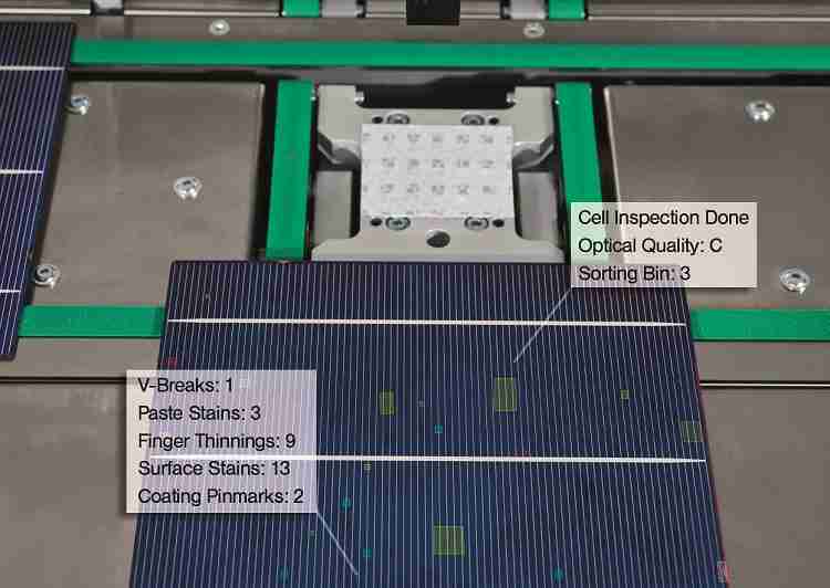 In contrast to BSF and PERC, heterojunction solar cells will require the optical inspection of new layer structures on both the front and the rear side, and introduce new grid patterns optimized for gluing or other low-temperature interconnection concepts.
The IBC cell, on the other hand, follows a different path. Even though shading is no longer important and contact structures may become larger again, the size of critical defects becomes smaller than ever, due to the dense arrangement and the interdigitated structure. Smallest defects which are invisible to the eye and which do not constitute optical quality issues can cause severe problems.The main risks are short circuits between the different contact regions, caused by fingers shifted to the side, fingers that are too wide and thus extend the contact area into the adjacent doping region, or bridging between two fingers.
IBC processing also introduces new materials to the solar cell process. Insulating paste is used to mask cell areas locally, and different kinds of metal paste are printed in layers. This requires careful inspection of the insulation layer for pinholes, as well as alignment checks between the different metal layers, which are all visible at the same time and have little or no contrast from each other.
Taking on the challenges: system, software and illumination
The overall requirements for AOI become more and more challenging. It is easy to adjust an inspection system to find a defect on a single cell under laboratory conditions. However, it is an entirely different matter to run the very same recipe in a challenging production environment – at speeds of 3600 cells/h and with thousands of cells showing varying defect contrasts – and at the same time yield consistent inspection results with overkill and underkill rates well below 1%.
 Dr. Christopher Berge studied Physics at the University of Hanover (Germany) starting 1992. He started his solar research career at the Institute for Solar Energy Research Hameln (ISFH) in 1997 in the group of Dr. Armin Aberle. After finishing university, he spent a year at ENEA, C.R. Casaccia, Italy doing research on optical coatings for UV applications, before returning back to photovoltaics by writing a Ph.D. Thesis at the Institute of Physical Electronics (now Institute of Photovoltaics) at the University of Stuttgart on the subject of monocrystalline thin film solar cells obtained from layer transfer, where he achieved a record efficiency for this type of cell.
After his PhD, Dr. Christopher Berge joined GP Solar GmbH, a daughter company of ISRA VISION AG, in 2004, where he is now Head of Product Management and responsible for the complete inspection product portfolio for wafer, cell, module and thin film.
As a leading global specialist for optical inspection, ISRA VISION / GP SOLAR is setting the standard for automatic process and quality control in the photovoltaic industry. Our innovative solutions for all photovoltaic applications, from wafers, cells and modules to thin film, solar glass and solar thermal, along with our worldwide service, offer our customers the highest performance and reliability in manufacturing.
Our new inspection technologies provide solutions for high efficiency solar cell production lines such as PERC, IBC, HIT, extreme thin contact fingers and new wire contacting designs. With this inspection technology, more than 2.5 GW of the latest innovative PV technology is already in production. Our state-of-the-art technology offers the perfect combination of production monitoring and detailed system inspection of all relevant process parameters, thus overcoming the main challenges in cell inspection. With extensive expertise in the field of automatic inspection solutions, we have stayed at the forefront of technological advances in the solar industry, as processes in the micrometer range become increasingly more important.
About ISRA VISION/GP SOLAR
ISRA VISION/GP SOLAR thoroughly explored the challenges for current and future solar cell production and carefully designed an inspection system that is capable of providing the right solution for all production technologies – stable, robust, with print editor and optional central recipe manager. “With ISRA’s illumination setup and multi-view technology, we were able to achieve maximum possible defect contrasts and stable inline performance at our customers’ lines, including shallow defects and at highest throughputs,” says Rüland. For IBC, a redesigned illumination setup makes the multi-view technology even more flexible and enables separate imaging of insulation layers and different metal layers. With ISRA VISION / GP SOLAR inspection systems, manufacturers benefit from an easy way to make their production future-proof and take on all the challenges arising from increasing price pressure and new cell designs.![]()


